Zeiss UltraPlus analytical FESEM
Ultra high resolution applications at low and high kV, EBSD, quantitative X-ray analysis, mapping, and variable pressure applications.
Facility
Contact
Contact
Contact
Contact
About
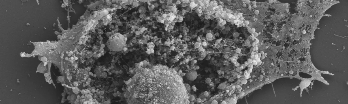
This FESEM is used for ultra high resolution application at low and high kV.
It is also used for electron back-scattered diffraction (EBSD), quantitative X-ray analysis, mapping, and variable pressure applications.
Features on this instrument include:
- Five-axis motorised stage
- Turbo and ion pump vacuum system
- In-lens and below lens secondary electron detectors
- Angular sensitive backscatter detector (AsB)
- Energy sensitive backscatter detector (EsB)
- Gas injection needle for variable pressure/charge compensation
- Oxford Instruments INCA x-act EDXA system, 10mm2 Silicon Drift Detector (ATW, 129eV)
- Oxford Instruments HKL EBSP
- IR Chamber scope
Training
All new users receive one-on-one training.
Attending the Introduction to Scanning Electron Microscopy workshop will give users a deeper understanding of SEM and help users to improve the quality of their data.
Applications
- CLEM (correlative light and electron microscopy)
- Electron back-scattered diffraction (EBSD)
- X-ray analysis and X-ray mapping
- High-resolution, low voltage imaging on non-conductive materials.