


Applications for materials science
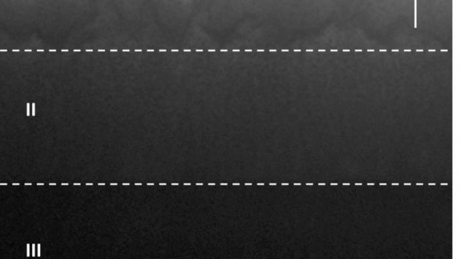
 Figure 1: Low magnification image of the Si0.1Ge0.9 film post ion implantation and annealing highlighting three distinct regions. The image was taken with the specimen aligned with the (110)Si direction parallel to the (001) plane of the film surface.
 (a) Typical grain boundary in region I, (b) Diffraction pattern from region I shows the ring pattern characteristic of a polycrystalline specimen, (c) Characteristic diffraction pattern from region II with specimen aligned close to the (110)Si zone axis
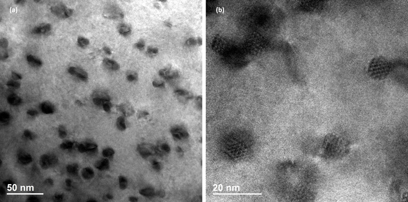
 Figure 3: (a) Detailed view of region II showing the In-rich precipitates present in this region. (b) The particles present a double Moiré pattern demonstrating that they are highly oriented.
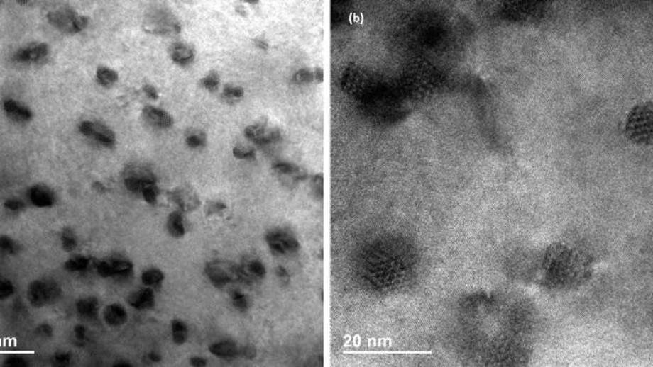 Figure 4: Details of the Si0.1Ge0.9/Si(001) interface. (a) Bright field image and (b) corresponding dark field image with the (002) vector excited highlighting the misfit dislocations resulting from the 3 % lattice mismatch between film and substrate.

In+ ion implanted Si0.1Ge0.9
Frequently in materials science, advanced techniques are used in order to improve the original properties of the starting material. In this example, In+ ions were implanted to increase the total charge carriers density of in the Si0.1Ge0.9 semiconductor film resulting in an increased conductivity.
Powerful characterisation tools are employed in order to better understand the final electronic behaviour, which is directly related to the final structure of the material. In this context, the transmission electron microscope (TEM) is a very versatile piece of equipment, allowing for observation of electron transparent samples (thickness typically of less than 100 nm) over a wide range of magnifications (50 - 1,500,000x magnification).
In this example, a low magnification image is displayed providing an overview of the ion implanted layer. It is possible to identify three different regions in the ~ 3 μm thick film after the process is finished. Region I is polycrystalline in nature and contain crystals as big as 0.5 μm. The second region is characterised by the presence of a large number of small nanocrystals, barely visible at this magnification.
Grain boundaries
Figure 2 shows a typical grain boundary in region I. In this example it is possible to see that the crystal on the left has a different crystalline orientation from the crystal on the right (Fig. 2(a)). Note also that it is possible to see the lattice fringes from the (111) planes in Si0.1Ge0.9 crystal.
Figures 2(b) and 2(c) show a comparison between the polycrystalline structure in region I (Fig. 2(b)) with the single crystal structure in region II (Fig. 2(c)).
Nanoparticle observation
Figure 3 displays a detailed observation of region II. At this magnification it is possible to identify the presence of In-rich nanocrystals inside the Si0.1Ge0.9 matrix. Surface energy minimisation process leads to the formation of faceted crystals with a cuboctahedron geometry.
Defect observation
Details from region III are better demonstrated in figure 4. In this region the lattice mismatch between the crystalline structures of pure Si and Si0.1Ge0.9 at the interface leads to the formation of misfit dislocations. By selecting the appropriate diffraction information it is possible to highlight the defects present in the specimen facilitating observation.
References
Ruixing Feng, Felipe Kremer, David J. Sprouster, Sahar Mirzaei, Stefan Decoster, Chris J. Glover, Scott A. Medling, John Lundsgaard Hansen, Arne Nylandsted-Larsen, Salvy P. Russo & Mark C. Ridgway.
Enhanced Electrical Activation in In-Implanted Si0.35Ge0.65 by C Co-Doping. Materials Research Letters, (2016).
R. Feng, F. Kremer, D. J. Sprouster, S. Mirzaei, S. Decoster, C. J. Glover, S. A. Medling, J. L. Hansen, A. Nylandsted-Larsen,S.P.Russo,M.C.Ridgway. Electrical and structural properties of In-implanted Si1−xGex alloys. Journal of Applied Physics 119, 025709 (2016).
R. Feng, F. Kremer, D. J. Sprouster, S. Mirzaei, S. Decoster, C. J. Glover, S. A. Medling, L. M. C. Pereira, S. P. Russo, and M. C. Ridgway Enhanced electrical activation in In-implanted Ge by C co-doping Applied Physics Letters 107, 212101 (2015).
R. Feng, F. Kremer, D. J. Sprouster, S. Mirzaei, S. Decoster, C. J. Glover, S. A. Medling, S. P. Russo and M. C. Ridgway. Structural and electrical properties of In-implanted Ge.Journal of Applied Physics 118, 165701(2015).

